- This is the series of "allowed" and "forbidden" energy bands that it y bands that it contains according to the band theory which postulates the existence of continuous ranges of energy values (bands) which electron may occupy "allowed" or not occupy 'forbidden".
- According to molecular orbital theory, if several atoms are brought together in a molecule, their atomic orbitals split, producing a number of molecular orbitals proportional to the number of atoms.
- However when a large number of atoms are brought together the difference between their energy levels become very small, such that some intervals of energy contain no orbitals and this theory makes an assumption that these energy levels are as numerous as to be indistinct.
Number, size and spacing of bands.
- Any solid has a large number of bands (theoretically infinite).
- Bands have different widths based upon the properties of the atomic orbitals from which they arise.
- Bands may also overlap to produce a bigger single band.
Valence and conduction bands
- Valence band is the highest range of electron energies where electrons are normally present at zero temperature.
- Conduction band is the range of electron energy higher than that of the valence band sufficient to make electrons free (de-localized); responsible for transfer of electric
charge.
- Insulators and semi-conductors have a gap above valence band followed by conduction band above it.
- In metals, the conduction band is the valence band.
Band structure of a semi-conductor.
- Electrons in the conduction band break free of the covalent bonds between atoms and are free to move around hence conduct charge
- The covalent bonds have missing electrons or 'holes'after the electrons have moved.
- The current carrying electrons in the conduction band are known as free electrons.
Doping of semi-conductors
- Doping is the introduction of impurities in semi-conductors to alter their electronic properties.
- The impurities are called dopants. Doping heavily may increase their conductivity by a factor greater than a million.
Intrinsic and extrinsic semi-conductors
- An intrinsic semi-conductor is one which is pure enough such that the impurities in it do not significantly affect its electrical behaviour.
- Intrinsic semi-conductors increase their conductivity with increase in temperature unlike metals.
- An extrinsic semi-conductor is one which has been doped with impurities to modify its number and type of free charge carriers present.
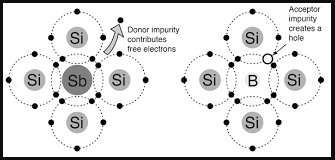
N-type semi-conductors
In this case the semi-conductor is given atoms by an impurity and this impurity is known as donor so it is given donor atoms (donated).

P-type semi-conductors
- The impurity within the semi-conductor accepts atoms with free electrons (dopants).
- This forms a 'hole' within the semi-conductors
Junction diodes
- Junction refers the region where the two types of semi-conductors meet.
- The junctions are made by combining an n-type and p-type semi-conductor.
- The n-region is the cathode and the p-region is the anode.
Forward bias of a p-n junction
- It occurs when the p-type block is connected to the positive terminal and the n-type block is connected to the negative terminal of a battery.
- The depletion layer of the junction reduces to be very thin to allow the flow of electric current.
Reverse bias of a p-n junction
- The negative terminal of the battery is connected to the p-type region while the n-type is connected to positive terminal.
- The depletion layer widens and resists the flow of electrons to minimal or zero (no current flowing through) when the electric field increases beyond critical point the diode junction eventually breaks down and at this voltage it is referred to as the breakdown voltage.
- Diodes are intended to operate below the breakdown voltage.


